3D visualization at nanometer scale by electron tomography
By combining advanced reconstruction algorithms with carefully optimized imaging conditions and tilt acquisition schemes, it becomes possible to visualize complex nanoscale structures in three dimensions (3D) while minimizing electron-beam-induced damage. This approach provides critical insights into structure-property relationships in materials that are difficult to investigate using conventional high-dose two-dimensional (2D) imaging techniques, enabling the study of increasingly complex functional nanomaterials.
For example, the helicity and three-dimensional morphology of chiral nanostructures can be accurately determined through 3D electron tomography, revealing structural information that cannot be unambiguously obtained from 2D projections alone.
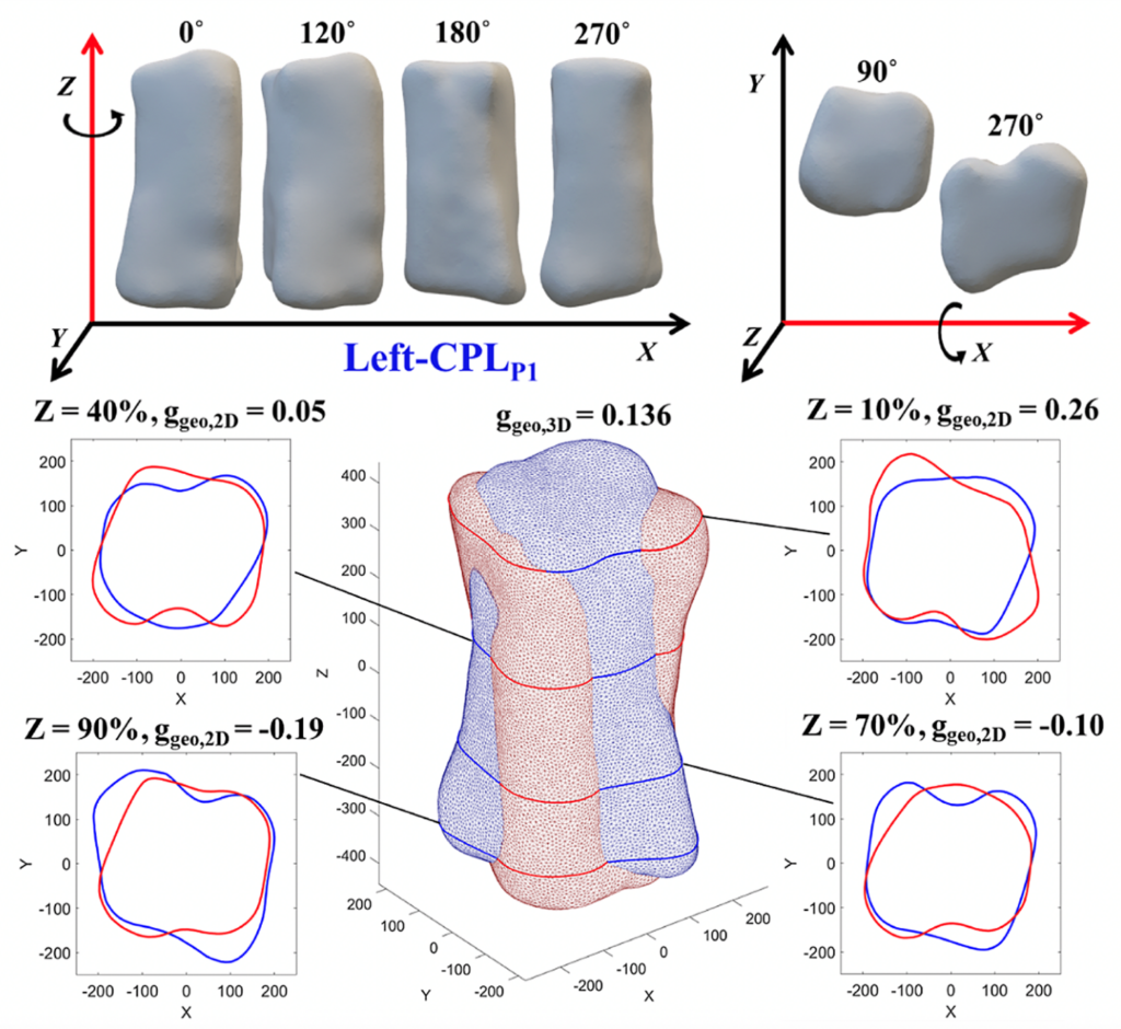
« Electron tomography results on post-CPL-illuminated-GRR NB morphology. (a) Snapshots of rotated (around the long axis) projections of an electron tomography 3D reconstruction of one of the left-CPL illuminated GRR experiments using 660 nm illumination with Au:Ag atomic ratio of 1:100 (labeled: Left-CPLP1). (b) Projections of the two ends of the same NB. (c) Geometrical analysis of the chirality of electron tomography 3D reconstructed shape of the same NB. The NB shape, shown in blue, was first displaced to coincide its center of mass with the origin, and the two largest eigenvectors of the inertia matrix of the NB were aligned with the Z- and Y-axes. Then the body was mirrored across the Z–Y plane with the resulting geometry shown in red. Four cross sections of the shape parallel to the X–Y plane are shown; demonstrating the asymmetry at four different Z-positions, with the 2D normalized chirality parameter value in each of them.«
Wanting He is currently a postdoctoral fellow at McGill University and is affiliated with the Facility for Electron Microscopy Research (FEMR). RQMEM is glad to take advantage of her expertise in transmission electron microscopy (TEM), electron energy loss spectroscopy (EELS), electron tomography and nanomaterials characterization.
She received her B.S. in Materials Science and Engineering from Beihang University and her M.S. in Materials Engineering from the University of Southern California. She earned her Ph.D. in Materials Science from the Institut National de la Recherche Scientifique (INRS), where her research focused on time-resolved ultrafast transmission electron microscopy (UTEM). During her doctoral studies, she investigated electron–photon–matter interactions using photon-induced near-field electron microscopy (PINEM), with particular emphasis on plasmonic nanomaterials.
To learn more about the electron tomography techniques, do not miss the upcoming webinar named Electron Tomography (ET) : Imaging 3D Nanostructure and Chemistry for Advanced Materials. The official presentation date will be announced soon. Consult our resources' page or subscribing to the Newsletter to stay informed. This webinar will be presented in English with French captions.
Electron tomography (ET) enables the three-dimensional (3D) reconstruction of nanostructures from a series of two-dimensional (2D) projections acquired over a range of viewing angles, providing significantly richer morphological and structural information than conventional 2D imaging. In this talk, Wanting He will introduce the electron tomography techniques developed at the Facility for Electron Microscopy Research (FEMR). These approaches enable 3D structural, chemical, and electronic property imaging of materials with nanometer and sub-nanometer spatial resolution.